
NVIDIA and MediaTek announced an unusual exchange on August 31. NVIDIA bought $3.5 billion in MediaTek convertible bonds. MediaTek agreed to adopt NVLink Fusion, giving its custom-silicon customers a route into NVIDIA’s rack-scale computing architecture.
The companies describe the arrangement as an expansion of work spanning AI infrastructure, local computing and automotive. The cloud piece carries the strategic weight: MediaTek will offer hyperscalers, cloud providers and frontier-model developers what the companies call a “prevalidated path” for connecting custom XPUs to NVIDIA NVLink systems, according to the joint announcement.
Customers get room to design processors around their own workloads. NVIDIA keeps control of the fabric technology that lets those processors behave as components of a larger AI system.
Control of that system boundary could outlast NVIDIA’s ownership of every compute die.
The XPU reaches the rack through a chiplet
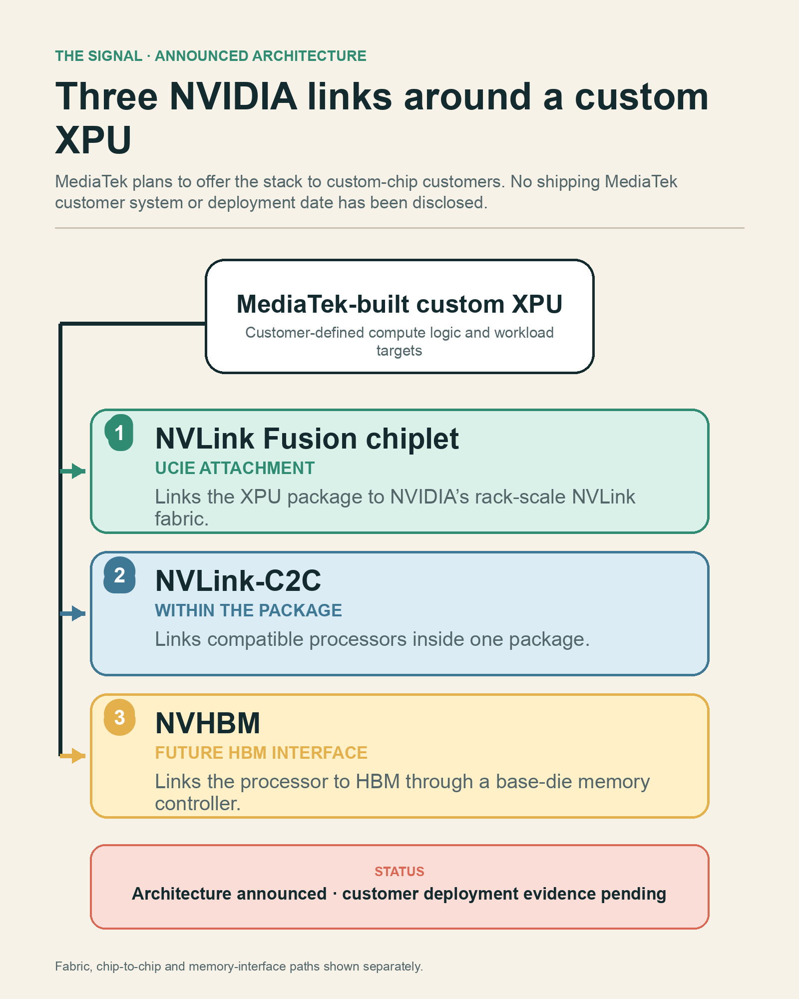
NVLink Fusion packages NVIDIA connectivity for third-party processor designs. MediaTek plans to make three pieces available to its customers: the NVLink Fusion chiplet, NVLink-C2C and NVHBM.
The Fusion chiplet is the center of the arrangement. ServeTheHome reports that a chip designer can attach it over UCIe and gain support for the NVLink fabric. The central NVLink components remain inside an NVIDIA-supplied black box instead of becoming IP that the customer directly implements.
Follow the path through a hypothetical MediaTek project. A customer defines the XPU’s compute architecture and hires MediaTek to build the custom silicon. MediaTek integrates NVIDIA’s Fusion chiplet beside that processor. The chiplet translates the XPU’s traffic into NVLink, giving the finished package a route to an NVLink network and NVIDIA rack-scale hardware.
NVLink-C2C covers short-range connections among chips. NVIDIA and MediaTek already used it in GB10, where it links components within the system-on-chip design. Under the expanded deal, MediaTek can apply the same connection technology to custom CPUs, multiple XPUs or other chip combinations, according to ServeTheHome.
NVHBM extends NVIDIA’s influence toward memory. ServeTheHome describes the new protocol as a way to connect processors to future HBM generations while placing the memory controller on the base die. Taken together, the three components cover package-scale connections, fabric-scale communication and a prospective path into high-bandwidth memory.
The resulting division of labor is precise. MediaTek and its customer control the specialized processor. NVIDIA controls the bridge into the larger machine.
Custom silicon becomes an NVLink participant
Hyperscalers build custom accelerators to tune cost, power use and workload behavior around their own services. A successful XPU can displace some general-purpose accelerator demand, creating an obvious tension for NVIDIA. The Signal’s earlier report on DeepSeek’s inference-chip project examined the same pressure from a model developer’s side.
NVLink Fusion gives NVIDIA another position in that procurement decision. A cloud operator can fund its own compute die and still choose NVIDIA networking, memory interfaces, GPUs or rack designs around it. NVIDIA collects architectural influence even when another company’s processor executes part of the workload.
MediaTek expands the reach of that approach. NVIDIA already offers NVLink Fusion directly to chip designers. The MediaTek agreement pushes access down to a custom-silicon partner that can design, package and deliver processors for customers, ServeTheHome notes. Each MediaTek engagement can now begin with an NVIDIA-compatible rack path among the available design choices.
That changes the operator’s build-versus-buy calculation. A custom accelerator project once implied assembling much of the surrounding system architecture or accepting another vendor’s proprietary stack. MediaTek can now offer differentiation at the XPU while preserving a route into NVIDIA’s rack environment, reducing the amount of integration work a customer must invent around the chip.
“Prevalidated” remains NVIDIA and MediaTek’s description rather than a demonstrated result. The announcement provides no named MediaTek customer, shipping system, benchmark, topology, pricing structure or deployment date for a custom XPU using the expanded stack. Operators should treat the claimed integration advantage as a design proposition until hardware and software tests establish it.
NVIDIA keeps the NVLink implementation inside its chiplet
A customer can own its accelerator architecture without owning the NVLink implementation that connects it to NVIDIA systems. NVIDIA’s chiplet may shorten development and integration work, but the published sources do not disclose licensing terms, access guarantees, support obligations or a migration path to another fabric.
Designing NVLink Fusion, NVLink-C2C or NVHBM into a package could increase the work required to change fabrics across packaging, verification, memory architecture and system software. The scale of that work cannot yet be measured, and the sources do not establish contractual lock-in. Buyers should require portability terms and estimate redesign scope before committing.
The supported strategic conclusion is narrower: custom processors can participate in NVIDIA rack-scale systems even when NVIDIA does not supply every compute die.
The $3.5 billion adds financial exposure to the partnership
NVIDIA purchased $3.5 billion in MediaTek convertible bonds, according to the companies’ release. Convertible bonds are debt that may convert into equity under specified conditions. The sources disclose no conversion terms, maturity, coupon, ownership outcome, governance rights or use of proceeds, so readers cannot infer an equity stake, control right or dedicated NVLink Fusion budget. The structure also resembles NVIDIA’s broader use of its balance sheet to support demand, described in The Signal’s analysis of a proposed OpenAI compute backstop, though the disclosed terms here do not establish the same commitments.
The technology partnership spans multiple Spark and automotive generations, while the NVLink Fusion work opens a custom-silicon channel. The evidence does not establish that the bonds finance those programs or bind either company to a specific custom-XPU roadmap. Buyers should evaluate product support and accountability from contract terms that have not been published.
GB10 provides prior engineering experience
MediaTek already occupies a substantial role inside an NVIDIA-branded processor. ServeTheHome reports that MediaTek was responsible for most of GB10’s development, including its CPU cores and memory controller, while NVIDIA supplied the integrated GPU and chip-to-chip connectivity. The joint announcement says GB10 powers NVIDIA DGX Spark. RTX Spark is described separately as an extension of the companies’ collaboration.
That prior project gives the new arrangement a credible engineering base. MediaTek has worked with NVIDIA’s connectivity and built silicon around NVIDIA components. The August 31 deal extends the relationship from a jointly developed NVIDIA product toward chips designed for MediaTek’s own customers.
The distinction expands the number of interests inside each project. GB10 had NVIDIA’s product requirements at the center. A custom XPU adds a third party with its own architecture, workload targets and procurement constraints. Repeating the GB10 collaboration pattern will require MediaTek and NVIDIA to support designs they did not originate and operational environments they do not fully control.
The companies are also continuing work on multiple generations of RTX Spark and DGX Spark chips, plus automotive platforms for software-defined vehicles, according to the joint announcement. ServeTheHome reports that MediaTek remains involved in planned Vera Rubin Spark and Rosa Feynman Spark generations. Those programs create repeated opportunities to refine the division between MediaTek’s system-on-chip work and NVIDIA’s compute and connectivity technology.
They do not establish that NVLink Fusion will perform cleanly in a hyperscaler’s custom rack. That evidence must come from the custom-XPU program itself.
Operators need answers at four boundaries
A buyer evaluating the MediaTek route should start with portability. Which parts of the XPU package can survive a future move away from NVLink Fusion, and which require redesign? The published material establishes UCIe attachment for the Fusion chiplet but gives no migration model.
Next comes operational ownership. MediaTek, NVIDIA and the customer will each control different parts of the stack. Incident response needs a single path across silicon behavior, package links, the NVLink fabric and rack integration. The August 31 announcement promises a prevalidated route without describing production support.
Software compatibility needs equal scrutiny. Both sources focus on hardware interfaces and system integration. Neither specifies compiler support, collective-communication behavior, orchestration, telemetry or how custom XPU software participates alongside NVIDIA accelerators. A connected chip still needs a usable programming and operating model.
Economics complete the review. Custom silicon can improve workload-specific efficiency, while an NVIDIA-controlled fabric may introduce licensing, component and system commitments. The supplied sources disclose the bond purchase and the available technologies, yet they provide no customer pricing or total-cost comparison. Procurement teams cannot infer savings from architectural flexibility alone.
The first disclosed MediaTek customer product will show how much processor freedom the arrangement permits while keeping the rack attached to NVLink.
Watch after September 2, 2026, for a named MediaTek custom-XPU customer, a tape-out or deployment date, published rack topology, software-support terms and measured performance across the NVLink Fusion boundary.
The Signal is the public edge of a private practice. Sherpa points the same intelligence engine at one owner's business — competitors, suppliers, regulators, watched daily, graded and sourced. Work with a Sherpa →